Basic Concepts
This section introduces the key concepts and terminologies that are essential in understanding the development and application of hwdbg.
High-level Terminologies
Different high-level terminologies are explained here.
Hardware Debugging
Hardware debugging refers to the process of identifying and correcting errors within electronic systems or reverse engineering hardware devices, such as microchips, circuit boards, FPGA IP cores, and other hardware components. Unlike software debugging, which deals with code, hardware debugging often requires the examination of physical signals, timings, and interactions within the hardware itself.
Field-Programmable Gate Arrays (FPGAs)
Field-Programmable Gate Arrays (FPGAs) are integrated circuits designed to be configured by the hardware designers after manufacturing. FPGAs are unique in their ability to be reprogrammed to perform a wide variety of tasks, making them a powerful tool in electronic design and testing. Their reconfigurability makes FPGAs ideal platforms for developing and deploying hardware debugging tools like hwdbg. Figure below illustrates the high-level architecture of FPGAs along with different components such as I/O Banks, Switch Matrices, CLBs, and Interconnect Wires.

Software Debugging Paradigms
Software debugging paradigms refer to the strategies, tools, and processes that are used to identify, trace, and fix software code errors. Common features in software debugging include breakpoints, stepping through the instructions, and inspecting variables. hwdbg aims to bring these concepts to hardware debugging and make hardware debugging more intuitive and efficient.
Signal Manipulation and Chip Fuzzing
Signal manipulation involves actively changing or interfacing with the logic signals within a designed logic or hardware to observe outcomes or induce specific states. Chip fuzzing is a form of testing that involves providing random data (referred to as fuzz input) to the inputs of hardware or the chip to uncover vulnerabilities or errors. These techniques are crucial in reverse engineering and security testing, allowing researchers to understand how hardware behaves under unexpected conditions or inputs.
Scope of Debugging
A key feature of hwdbg is its ability to be synthesized into FPGAs (at this stage it only supports AMD Xilinx FPGAs). This means that the debugger can be implemented into FPGAs, enabling hwdbg to run directly on hardware for real-time debugging and testing. This capability is important for testing high-frequency signals (at the speed range of FPGAs) and for scenarios where a simulation does not capture the full spectrum of potential hardware behaviors. More importantly, this debugger is designed to debug chips in a black-box scheme and assumes that the source code of the chip or the IP core is not available.
Debugger Customizability
hwdbg is designed to be highly customizable and open-source. Customizability allows users to adapt the debugger to their specific needs, enhancing its utility across various hardware designs and applications. For example, the user is able to customize the number of input or output pins as well as the number of samples that need to be gathered from the debugging device.
Input to Debuggee
Inputs for hwdbg can be provided through various means including direct user input via command-line interfaces, script files containing test cases or debugging instructions, and automated testbench setups that simulate specific conditions or inputs to the hardware under test. Moreover, in a real debugging scenario, the chip/IP core pins are connected to the inputs/outputs of the hwdbg and this way, the debugging of the signals are possible through this debugger.
Debugging Modes
There are two general modes of debugging in this debugger, Passive Debugging, and Active Debugging.
Passive Debugging
In this debugging mode, hwdbg acts as an introspection tool, and monitors different signals to the target debugging module.
Active Debugging
In this debugging mode, hwdbg is able to both monitor and manipulate signals (Input/Output). These signal modifications are configured by the user's custom scripts.
Technical Terminologies
Here, the technical terms used in this debugger are explained.
Programmable Logic (PL) and Processing System (PS) in FPGAs
In FPGAs, the Programmable Logic (PL) and Processing System (PS) are two main components that work together to provide a flexible hardware platform. The PL (also referred to as the FPGA part) consists of configurable logic blocks, interconnects, and other resources that can be programmed to implement custom digital circuits and functions. This allows designers to create highly customizable hardware accelerators, interfaces, and processing pipelines to meet the specific requirements of their applications. On the other hand, the PS (also referred to as the processor) is a pre-designed processing element such as an ARM processor as well as memory controllers, and peripheral interfaces. The PS provides general-purpose computing capabilities and supports standard software development tools and operating systems (e.g., Linux). By integrating the PL and PS within the same FPGA device, designers can create heterogeneous systems that leverage the strengths of both hardware and software processing paradigms. This combination enables a wide range of applications, from high-performance computing and signal processing to embedded systems and IoT devices, making FPGAs a powerful platform for the deployment of custom hardware solutions. Figure below depicts PS <> PL and connection components of Zynq 7000 FPGAs.
Partial Reconfiguration
Partial reconfiguration is a relatively new feature of FPGAs that allows specific regions or modules of the FPGA to be reconfigured dynamically while the rest of the device remains operational. This capability enables on-the-fly modifications to the FPGA configuration, without the need to reprogram the entire device. Partial reconfiguration is used in different parts of hwdbg mainly to satisfy the needs for executing different custom scripts.
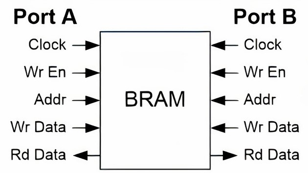
Block RAM (BRAM)
Block RAM (BRAM) is an SRAM resource within FPGAs that provides high-speed, on-chip memory storage. BRAMs are fabricated into configurable blocks that can be instantiated and interconnected within the FPGA fabric to meet the memory requirements of a design. They offer several advantages over external memory solutions, including lower latency, higher bandwidth, and reduced power consumption. BRAMs support various read and write modes, as well as dual-port and distributed memory configurations. In hwdbg, a Block RAM is shared between PL and PS and the debugger communicates with PL by using this shared block RAM (e.g., send configuration commands). Figure below shows input/output ports in a dual-port BlockRAM (similar to the BRAM component used in hwdbg).
Advanced eXtensible Interface (AXI) Protocol
AXI (Advanced eXtensible Interface) is a widely-used protocol in FPGA-based systems for high-performance communication between IP cores and memory-mapped peripherals. Table below depicts different types of AXI protocol.
| Protocol | Description |
|---|---|
| AXI4 | AXI4 (Advanced eXtensible Interface 4) is the most commonly used variant of the AXI protocol. It features separate read and write channels, support for multiple transactions, burst transfers, and advanced features such as QoS (Quality of Service) and address tagging. |
| AXI-Lite | AXI-Lite is a simplified version of the AXI protocol designed for lightweight and low-bandwidth communication between the master and slave components in an FPGA-based system. Unlike AXI4, AXI-Lite supports only single-beat transactions, does not include burst transfers or multiple transactions, and has reduced signaling requirements. |
| AXI-Stream | AXI-Stream is a specialized variant of the AXI protocol optimized for streaming data transfers, such as audio and video processing, signal processing, and data streaming applications. Unlike AXI4 and AXI-Lite, which use separate channels for read and write operations, AXI-Stream employs a single unidirectional channel for data transfer. |
MIO and EMIO
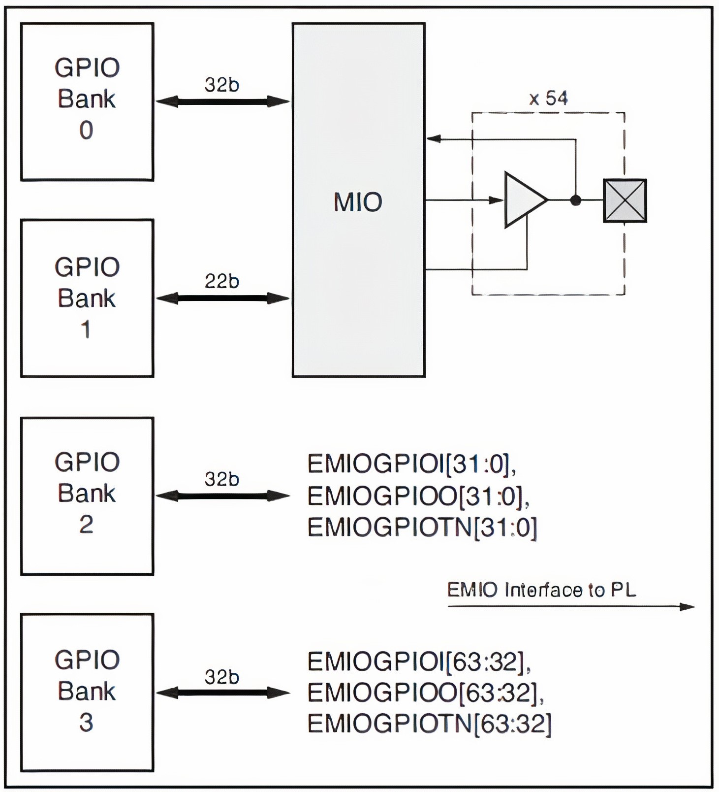
The PS and PL can be connected through multiple interfaces to make integration between the processor, peripherals, and the FPGA fabrics. Using these connections, PS can access resources in the PL or access to the data of different GPIO ports, or send data to the PL. The PS I/O peripherals, including the static/flash memory interfaces, share a multiplexed I/O (MIO). These pins are used to connect different GPIO Banks to the PS. There is also another type of connection called extended multiplexed I/O interface (EMIO) which is used for connecting PS directly to the PL. In hwdbg, EMIO ports are used to notify the PL (from PS) about the occurrence of a special event.
Generic Interrupt Controller (GIC)
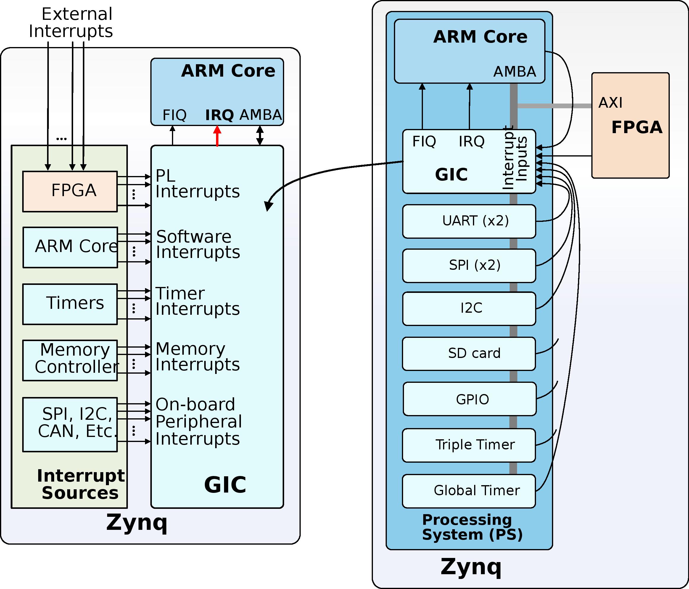
The Generic Interrupt Controller (GIC) handles different shared interrupt sources, including IP implemented in the FPGA fabrics and dedicated peripherals. Each CPU has multiple external peripheral interrupts as well as internal peripheral interrupts. An interrupt controller multiplexes a number of possible interrupt sources on the platform for presentation to the processor. Once an interrupt is triggered, the generic interrupt handler calls an Interrupt Service Routine (ISR) and executes whenever a processor receives an interrupt request. This routine chooses which interrupt to handle by reading the Interrupt Controller registers, acknowledges the Interrupt Controller, and launches the specific interrupt handler. Figure below illustrates different components and sources of the GIC controller in ZYNQ FPGAs. hwdbg uses interrupts as a way of communicating from PL to PS, whenever an event happens that requires an action from the processor, the interrupt line goes high, indicating that the PL needs to inform PS about a special event.
Previous Works
The domain of hardware debugging has witnessed significant advancements, driven by the need for more efficient and reliable debugging tools. Various methodologies and tools have been developed to address the challenges associated with hardware debugging, including side-channel attacks, synchronization issues, and verification. This section provides an overview of the key developments in hardware debugging technologies and highlights their relevance to the hwdbg hardware debugger.
Side-Channel Attack Mitigation
Side-channel attacks pose a significant threat to hardware security, exploiting physical caveats such as power consumption, electromagnetic emissions, and timing information to extract sensitive data. Tools like ChipWhisperer and Riscure's Inspector have been developed to facilitate side-channel analysis and testing. ChipWhisperer, for instance, integrates hardware and software to perform side-channel attacks and analyze vulnerabilities in cryptographic implementations. The hwdbg debugger builds on these concepts by incorporating robust mechanisms to monitor hardware using different sensors, ensuring enhanced security in hardware designs.
Communication and Signal Interception
Synchronization between different components of a hardware debugger is crucial for accurate data capture and analysis. The OpenCores project provides a repository of open-source hardware modules, including synchronization modules that ensure seamless data flow between different parts of the system. Similarly, the hwdbg debugger employs a sophisticated synchronization module that manages the timing and coordination of data transfer operations, preventing data loss and maintaining the integrity of the debugging process.
Efficient interception of signals is essential for real-time hardware debugging. Tools like Xilinx's Integrated Logic Analyzer (ILA) and Intel's SignalTap provide in-depth signal analysis and data processing capabilities, which allows developers to monitor and interpret signal activities within FPGAs and other programmable devices. The hwdbg debugger enhances these capabilities by incorporating an advanced interpreter module that processes incoming signals, determines the appropriate actions, and generates responses accordingly, thus streamlining the debugging workflow.
Hardware Monitoring and Logic Analyzers
When it comes to hardware debugging, several tools and IP cores designed for monitoring and modifying signals on-the-fly play a key role in enhancing debugging capabilities. One notable example is PHMon (Programmable Hardware Monitor), which provides a flexible and programmable platform for monitoring hardware events in real-time. PHMon allows for the dynamic observation and manipulation of hardware signals, enabling developers to identify issues without halting the system. This tool leverages a combination of hardware and software to provide detailed insights into system behavior, making it a valuable asset in the debugging toolkit. Other than that, researchers previously tried to bring the concepts of software to hardware testing like fuzzing and it is proven that software techniques and concepts are effective in hardware.
Additionally, frameworks like Xilinx's Vivado Debug IP and Intel's FPGA Debug and Monitoring IP Cores offer comprehensive solutions for real-time hardware monitoring and control. These IP cores integrate seamlessly into FPGA designs, providing capabilities for capturing and analyzing signal activities. Vivado Debug IP, for example, includes features such as the Integrated Logic Analyzer (ILA) and Virtual I/O (VIO), which enable on-chip debugging and real-time signal manipulation. Similarly, Intel's SignalTap Logic Analyzer allows developers to monitor internal signals and adjust them as needed during runtime, facilitating immediate feedback and debugging.
Furthermore, proprietary solutions like ARM's CoreSight technology provide extensive debugging and trace capabilities for ARM-based systems. CoreSight includes components like the Embedded Trace Macrocell (ETM) and the Instrumentation Trace Macrocell (ITM), which support detailed tracing of program execution and data flow. These components enable developers to monitor and modify signals at the clock cycle granular level, aiding in the identification of bugs and performance bottlenecks. Similarly, hwdbg aims to provide control over hardware, enabling monitoring and modification of signals down to the granular level of a single clock cycle.
At last, hwdbg hardware debugger represents a comprehensive solution that integrates advanced features from various state-of-the-art tools and methodologies. By addressing side-channel vulnerabilities, ensuring synchronization, facilitating efficient packet interpretation, and incorporating sensors, hwdbg offers a robust and reliable platform for hardware debugging.