Design Flow
Figure below shows the flowchart of hwdbg from design to the bitstream generation for FPGA implementation. It starts with HDL code, which can be written in Verilog (.SV) or SystemVerilog (.V). This code is then synthesized by Xilinx Vivado into an RTL netlist (.rtl).
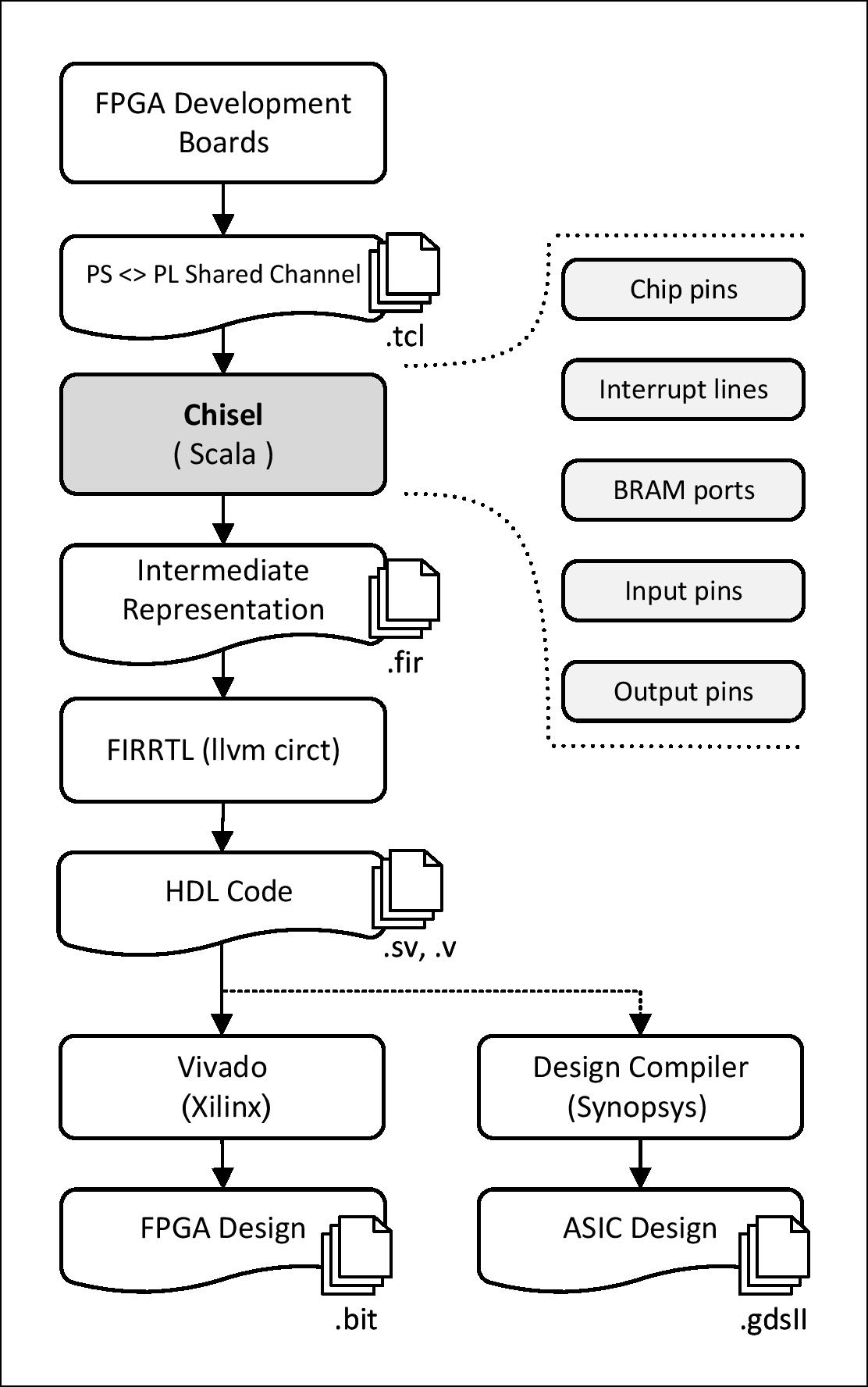
Next, the RTL netlist is simulated using a simulator like ModelSim. This simulation helps to ensure that the design is functioning as expected. After simulation, the design is translated into a bitstream file (.bit) using Vivado. This bitstream file is then loaded onto the FPGA development board.
The FPGA development board contains a programmable logic device (PLD) that can be configured to implement the design. The bitstream file tells the PLD how to connect its internal logic blocks to implement the desired functionality.
The FPGA development board also includes a processor system (PS) that can be used to control the PLD. The PS and PLD can communicate with each other through a shared channel. The PS can also communicate with the outside world through the chip pins.