The Sender/Receiver Synchronization Module
This module plays a crucial role in ensuring that the sending and receiving operations within the hwdbg occur without conflicts. It manages the timing and coordination between the sending and receiving modules, preventing them from attempting to access the shared resources simultaneously. Other than that, based on the fact that Xilinx FPGAs are manufactured with BRAMs with two ports, one port is shared with PS, and the other one is shared with PL, thus, no two modules (in PL) can use a single port simultaneously. By enforcing synchronization, this module helps prevent data corruption between multiple modules (in PL) and ensures the integrity of communications between the debugger and the PL/PS.
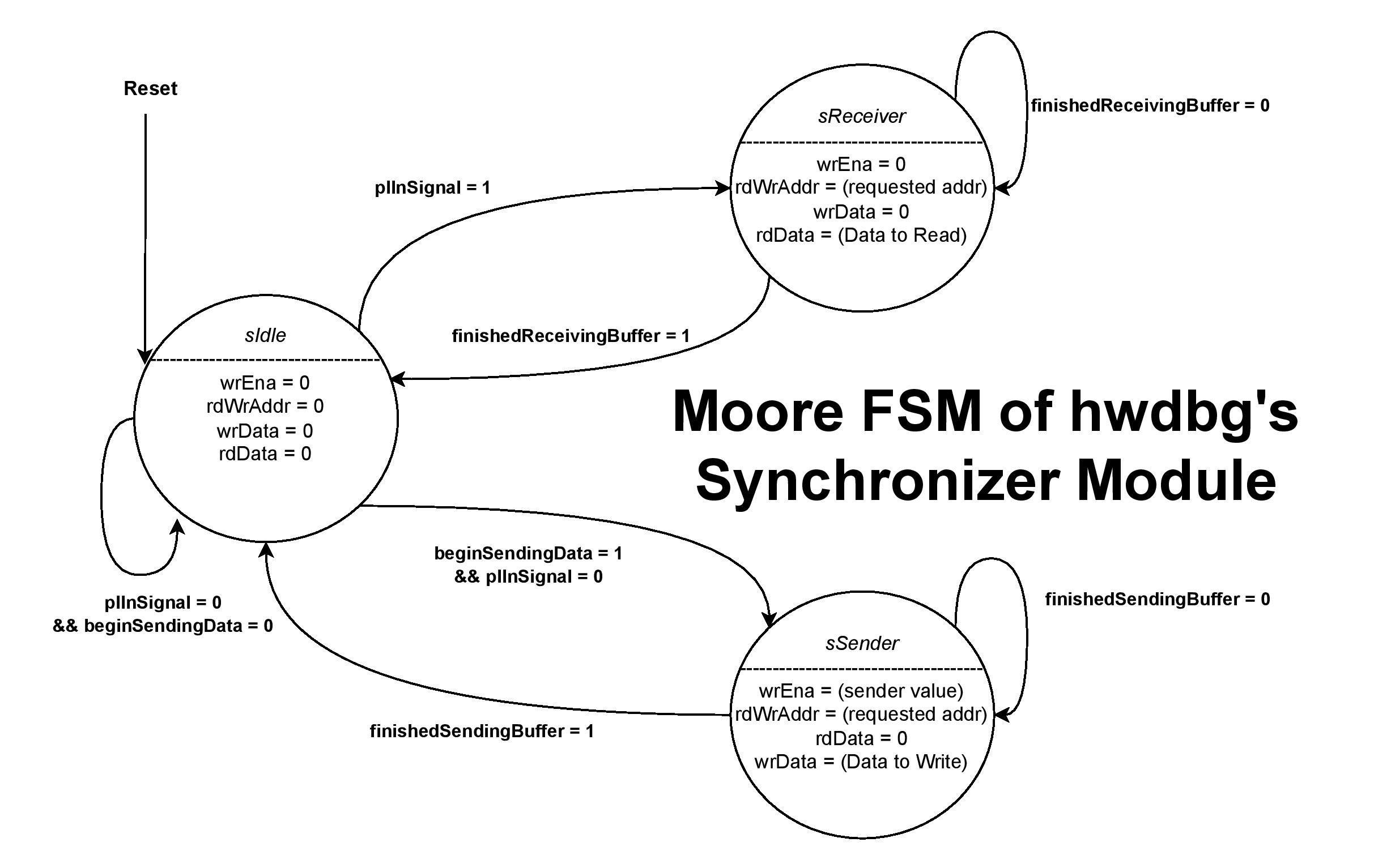
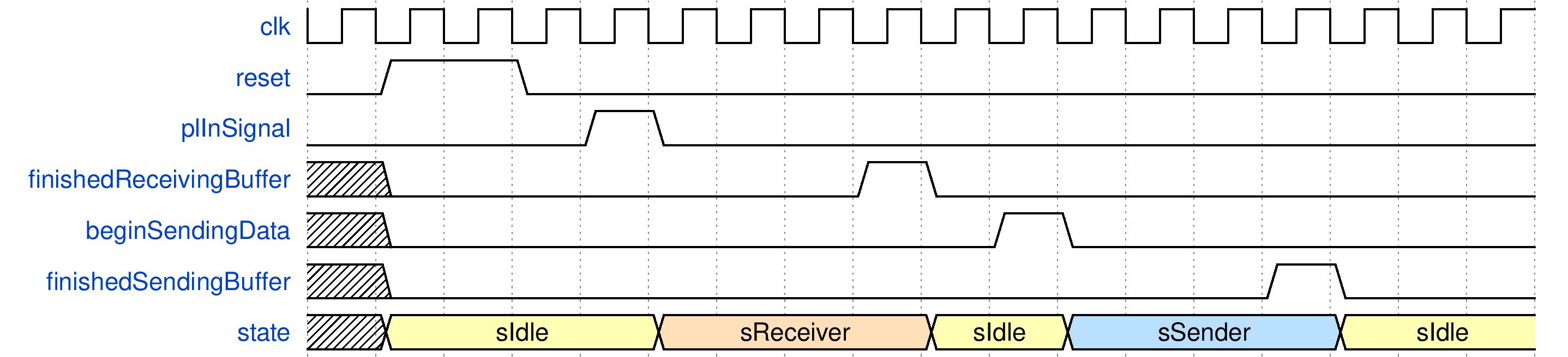
The diagram illustrates the Moore FSM and the figure is the waveform of the synchronizer module in the hwdbg hardware debugger, responsible for coordinating the sending and receiving of data. The FSM begins in the sIdle state, where all control signals (wrEna, rdWrAddr, wrData, rdData) are initialized to zero, awaiting a trigger to commence data operations. When the pllInSignal is asserted (pllInSignal = 1), the FSM transitions to the sReceiver state, where it performs data reading tasks. In this state, the address for reading is set (rdWrAddr = requested addr), and the data to be read is managed. The module remains in sReceiver until the finishedReceivingBuffer signal is set, indicating that the data reception process is complete.
Following the reception, the FSM moves back to the sIdle state until conditions for sending data are met (beginSendingData = 1 and pllInSignal = 0). Once these conditions are satisfied, the FSM transitions to the sSender state. In sSender, the module is configured to enable writing (wrEna = sender value), set the address for writing (rdWrAddr = requested addr), and prepare the data to be written (wrData = Data to Write). The FSM remains in this state until the finishedSendingBuffer signal is asserted, which marks the completion of the data transmission. Finally, the FSM returns to the sIdle state, ready for the next cycle of operations. This synchronized process ensures efficient and orderly data handling, maintaining the integrity and reliability of data transactions within the hardware debugger. Note that in hwdbg, receiving command precedes sending data.